Stiffler Scientific
Dr. Ronald R. Stiffler

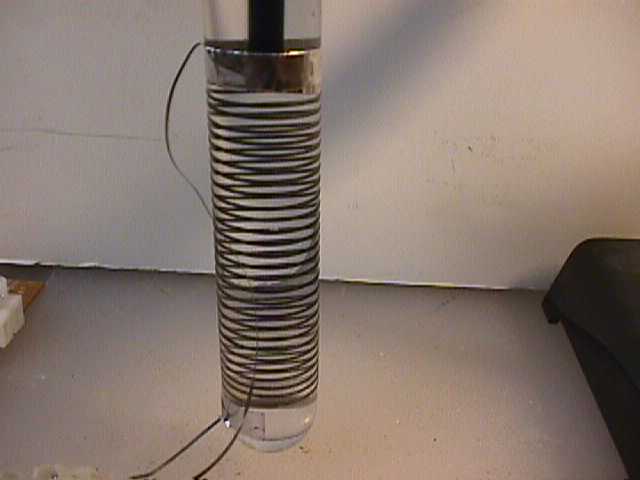
A test tube with a resistive inductor (RL) wrapped around the exterior.
Fig: 1
The test tube is filled with 20-25mL of
distilled water.
You can see a glass thermometer bulb at top of test tube. Note
that no stirrer is being used. With
only 20-25mL of water in the tube and the
thermometer placed at the top in the last ~5mL there
should not be a
significant gradient and a slight shaking of the tube at the end of a test run
will mix
the water so that the temperature difference is relatively
uniform.
*The glass thermometer was initially used and later replaced
by LM335's that were calibrated before
each run to a NIST traceable
standard.
Fig: 2

The Pyrex glass test tube with its Nickel Chromium coil.
Fig: 3

The following shows how it will fit together inside the calorimeter.
Fig: 4

The basic parts of the Calorimeter.
Fig: 5
Each side is cut out for the test tube. On
the right foam section a plastic sleeve for
thermometer to pass
through is added and glued to the foam. This makes for a tight fit and
reduces
energy loss.
Fig: 6
What the assembled Calorimeter looks like.
Fig: 7
The Cell as it is mounted inside the
Calorimeter and a cutout for the connector is made into one side
of the foam.
To aid against leaks, glass cotton is placed over the cell before the sides are
enclosed
around it.
Fig: 8
The Cell assembled and ready for testing.
Fig: 9
If you do not want to go to the small
expense of using the block foam (total cost ~ $10US) for the calorimeter
you can us
Hot & Cold Styrofoam cups along with the test tube and water.
Whatever method you use should perform well and provide
only a small margin
of error, if properly calibrated and proper measurement during the
testing. One must always
allow for and take into account the glass of the
test tube and surrounding air space inside of the cup arrangement.
Once this is done properly, very accurate measurement
can be made.
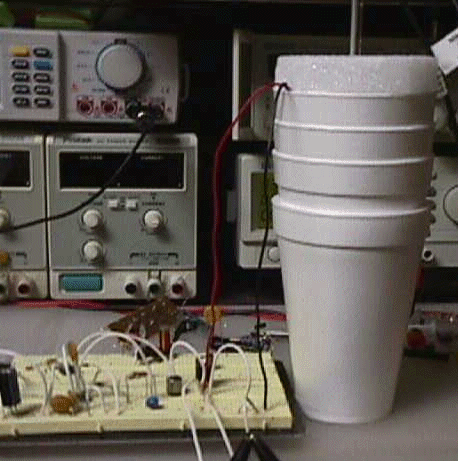
*The usage of cups was found to have serious limitations. As
seen in the following example (4) cups, each inside of the other
with the
bottoms cut out to allow for the test tube length, a foam cap and glass cotton
in the bottom cup. In short, the cups are
poor insulators. Once the
water reached a temperature of ~36'C one could feel the heat on the exterior of
the cups and the
temperature curve begins to level out as the heat flows into
the ambient environment. I was unable to sustain a CEC>1 once
the
temperature reached 42'C. From this point on the CEC gradually declined
to where it leveled at around 83%.
Fig: 10

|
It should be noted that there should be no interaction from the (pure?) ceramic core on which the 'Rosemary Ainslie' original tests were performed. Because the ceramic should not interact with her 'Magnetic Model', the tests being performed here which use a Pyrex Glass rather than Ceramic for the coil form (water container) should not play a significant part in the measurement results. The tests I am performing will follow a similar protocol to the originals by 'Ainslie', but I am using an Adiabatic enclosure and applying the resulting heat to 20-25mL of water inside of the test tube. *All energy readings that contain AC components are taken by signal integration at a 40MHz-sampling rate. All oscilloscope readings are either referenced to ground or taken with differential probes without ground reference. Sampling is performed across Composition Carbon resistors of low value (0.1 - 1.0 ohms) to remove inductive and phase differentials. First Run Observations Initially I set out to obtain a set of driver (operational) frequencies close to the inventors' specifications. The driver circuit was a conventional 555 CMOS timer chip that was wired in a PWM (pulse width modulation) configuration. The same supply voltage was used for the 555 and the MOSFET output stage (12V). Fig: 11
In figure (11) one sees a long discharge time in the gate capacity and this needed to be changed and was a result of engineering convention where I was using a 110K resistor from the Gate to ground. Removal of this resistor allowed for a rapid discharge back through the 555. In the images of Fig: 12 once can see a trailing spike on the Gate of the MOSFET and this is on the Gate side of the Gate drive adjustment resistor. The Drain shows a normal ring down from the inductor and the large initial peak. The Drain HV peak is masked in the display as the Gate and Drain are overlaid in the picture. Fig: 12
MOSFET Oscillations Under certain conditions I have observed oscillations on the Gate and Drain of the MOSFET. These oscillations do not match any of the Ainslie Documentation and are orders of magnitude higher than described. Because of their strange nature I felt is necessary to look further into what was taking place and if the oscillation was an advantage or disadvantage over the lower frequencies described by Ainslie. Fig: 13
Fig: 13
As I work with the circuit and slowly move to what the original specification was I find many interesting things. The most interesting was when I split the power supplies between the 555 and the MOSFET. In the following trace one can see a HV spike of 149V and a continuous ring down during the 'OFF' drive cycle. The spike integrates to very little energy, although the1.49MHz ridding on the 20V supply voltage integrates with interest. FIG: 14
Fig: 15
There is a significant amount of discussion with regard to a returned energy pulse to the power supply (usually battery) from the collapsing field of the inductor in the 'Ainsile' circuit that offsets the energy supplied by the powering source. This of course is nothing new and in many AC circuits can be explored by the insertion of a small valued resistor in series with the supply and integrating the waveform. The significance of this reducing pulse appears to be insignificant when compared to the overall Heat production issue. Looking at the following diagram will allow for a better explanation of why I have made this determination. Fig: 16
In my explanation I make the following assumptions for simplicity. V1 is a battery, it shall be a Lead Acid type of 24
Volts Now lets explore the conditions under which a pulse of
energy could return to the battery when the field of L is charged during
an 'ON' pulse followed by an 'OFF' pulse. If there is not connection
through M1 in order to complete a path back to the battery, any current
would be totally one sided which is not possible and if it were the actual
energy content would be very small as the current would also have to flow
through the resistance R. What I have confirmed is that the field collapse
supplies a current that does indeed heat the coil (RL) and the diode (D1),
but does not return energy to the battery. If we assume M1 as a very high resistance (remember the pulse is < 1kV so the intrinsic diode is not conducting), then some small signal could flow through the high resistance of M1, but the pathe (return) is by way of Cx and not the battery. As it now stands I see no significance in considering any returned energy, rather it should be considered as a mere reduction of energy drawn during portions of the operational cycle. Addressing the heating issue is a bit different, yet a modification needs to be made to the original circuit. A second inductor is added.
Fig: 17
Fig: 18
Fig: 19
|