A tutorial on switching-mode power supply design by Jerrold Foutz
The primary advantage of switching-mode power supplies is they can accomplish power conversion and regulation at 100% efficiency -- given ideal parts. All power loss is due to less than ideal parts and the power loss in the control circuitry. In this section we explore some of the switching-mode power supplies that can be constructed using only one each of the parts from our simple parts list.
One of the simpler switching-mode power supplies is one that is used to control a heater. For example, an inexpensive space heater I have applies full household ac voltage to a heater element when the temperature is less than that set by a simple thermostat and turns the ac power off when the temperature is above the set point. The heater turns on and off every several minutes to keep the room temperature constant. Closer to our example might be a heater in a crystal-oscillator oven used to keep the temperature of the crystal within narrow limits. For this circuit, we only need to use the switch from our list of components. The schematic is shown in Figure 3-1.
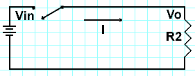
Figure 3-1: Heater Schematic
As with our previous examples, Vin is 12 Vdc and the load resistor R2 is 0.25 ohms. The objective is to open and close the switch so that the average voltage across R2 is 5 Vdc. The waveform of the voltage across R2 is shown in Figure 3-2.

Figure 3-2: Heater Waveform
This is the first waveform we have encountered in this tutorial. In your design of switching-mode power supplies you will have to work with many waveforms and calculate properties such as period, frequency, duty cycle, harmonics, average and rms (root-mean-square) values -- both with and without the dc component, etc. Unless you really like solving definite integrals and doing Fourier analysis, you will want a handbook that gives you characteristics of common pulse and periodic waveforms.
In Figure 3-2, the period, T, of the waveform is Ton + Toff, and by definition, the reciprocal of the period is the frequency. For example, a period of 50 us results in a frequency of 20 kHz. The ratio of Ton/(Ton + Toff) is called the Duty cycle, D, -- a parameter much used in switching-mode power supply calculations. The average value of the waveform over a period is shown by a dotted line.
For those who have had calculus you will remember the average value of a function is (1/T)*(Integral zero to T of the function). In this case you have to evaluate the integral from 0 to Ton and from Ton to T and add them. Or you can look it up in a handbook and see the average is Vin*D.
Again, those with calculus know to get the RMS (Root-Mean-Square) of a function you first square it and then take the mean or average of the result as before. You then take the square root to get the answer. Or you can look it up in a handbook and see the RMS is Vin*SQRT(D).
Example:
Vin = 12 Vdc
Vo = 5 Vdc (average)
D = (5 V)/(12 V) = 0.417
Vrms=(12 V)*SQRT(0.417) = (12 V)*0.645 = 7.75 Vrms.
Iaverage = (0.417)*(12 V)/(0.25 ohm) = 20 A
Pin = (12 V)*(20 A) = 240 W
These are the answers we got in our series and shunt regulator examples and are no surprise.
We might expect that the power in R2 is the same as before, (5 V)*(20 A) = 100 W, but that doesn't make sense, since we are taking 240 W from the source and there is nowhere it can go except into R2. Recalling that power in a resistor is (Vrms)*(Vrms)/R, and the rms voltage is 7.75 Vrms, then we get (7.75 Vrms)(7.75 Vrms)/(0.25 ohms) = 240 W in R2, and everything balances.
Notice that the rms value of the waveform is higher than the average value. This is true in all duty cycle controlled switching-mode power supplies. Also notice that all the power taken from the source is delivered to the load assuming ideal components. This will be true in all the examples discussed in this section, however, there is one notable exception. The exception is if you try to switch directly into a capacitor, which we discuss next.
From our parts list we will add a capacitor to our heater circuit and get the schematic shown in Figure 3-3.
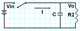
Figure 3-3: Switched Capacitor Converter
One might erroneously argue that the only dissipative element in this circuit is the load and all energy from the source goes to the load. Therefore if we control the switch to maintain 5 Vdc on the capacitor we have a 100% efficient converter. This is not the case since charging a capacitor directly from a voltage source or capacitor dissipates as much energy as is transferred to the capacitor. This problem, Energy Loss in Charging a Capacitor, is discussed in the problem section of the SMPS Technology Knowledge Base. Since you will see this circuit in many variations throughout your design career, it is well to recognize it and understand it. This circuit has it uses, but high efficiency power conversion from a source that is significantly different from the output is not one of them. In order to keep the voltages near each other and increase efficiency, many applications switch topologies during operation (e.g. from a voltage doubler to a tripler) to improve the efficiency of this circuit.
From our parts list we will add an inductor and diode to our heater circuit and get the schematic shown Figure 3-4.

Figure 3-4: Switched Inductor Converter
Unlike our capacitor example, this circuit is 100% efficient with ideal components. It's major problem is terrible load transient response. If the load is removed, the current must continue to flow in the inductor and the output voltage tends to go to infinity. If the load is increased by two, the output voltage is halved, since the inductor current remains the same until adjusted by the L/R time constant. Because of the terrible load transient response this circuit is rarely used as a voltage regulator. But it is interesting to note that in the type of dc-dc converter we are discussing in this section, an inductor is always needed, but a capacitor is not. It is also interesting to note that this is the equivalent circuit of a switching-mode control of current in a motor field winding, which is represented as an inductor and series resistor.
Note that the diode is necessary to provide a current path for the inductor current when the switch opens. Otherwise the voltage across the inductor would build up to several hundred volts until the energy stored in the inductor would dissipate as an arc in the switch, charge the parasitic capacitance of the inductor windings, or result in some other undesired phenomenon.
A rule of thumb, which we will use later for selecting a value of inductance in an LC filter, is to start with an inductor value that results in a peak-to-peak inductor current that is 10% of the full load current. For our example of a 12 V input, 5 V output, 20 A load, and 20 kHz switching frequency, the inductor can be calculated from the formula V = L*(di/dt). This is a formula you will constantly use in switching-mode power supply design, hence worth memorizing.
Example:
L = V*Ton/I
V = 12 V - 5 V = 7 V
Ton = D*T = 0.417*50E-6 = 20.85E-6
I = 20 A * 10% = 2 A
L = (7 V)*(20.85E-6 s)/(2 A) = 72.3 uH
=> 75 uH
The resulting two amps (1.94 A) peak-to-peak ripple current gives about a half volt peak-to-peak ripple current in the 5 V, 20 A load. Note that you can decrease the ripple current to as small as you want by increasing L, or make L smaller by allowing more ripple current.
From our parts list we will add a capacitor to our switched inductor converter and get the buck converter as shown in Figure 3-5.
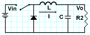
Figure 3-5: Buck Converter
The buck converter goes by many names, voltage step-down converter, current step-up converter, chopper, direct converter, et .al. No matter the name, converters derived from this topology account for a substantial percentage of all converters sold. Understanding its operation is basic to switching-mode power supply design.
Our first problem is to select initial values of L and C. Later the design can be optimized. In our switched inductor example we used the rule of thumb of designing L to get a peak-to-peak ripple current of 10% of the full load output current and got a value of 75 uH. We will use overshoot to get a value for C and then check the output ripple.
The problem of overshoot, Output Filter Design - Overshoot, is discussed in the problem section of the SMPS Technology Knowledge Base and it is an important consideration in output filter design -- enough so that it is prudent to consider overshoot first, rather than output ripple as is normally done, so that overshoot is not forgotten. We will use a simple rule of thumb of making the characteristic impedance of the filter, Zo, equal the load resistor, which gives an overshoot of SQRT(2)= 1.41 and a slightly over-damped filter at full load. For our example, if our full load 20 A is removed, the 5 Vdc voltage goes to (5 V)*1.41 = 7.07 V.
Solving Zo=SQRT(L/C) for C = L/(Zo*Zo) = 75E-6/(0.25*0.25) = 1,200 uF
In checking for ripple we will use another formula that is used enough in switching-mode power supply design that it is worth memorizing, V = (1/C)*INTEGRAL( i(t)*dt), which combined with V=L*(di/dt) allows us to calculate output ripple due to the capacitor capacitive impedance (which is often less than the contribution of capacitor equivalent series resistance (ESR) to output ripple).
Example:
Solving for current as a function of time in the output capacitor
The current in the capacitor is the triangular current in the inductor which
has the slope K
K = di/dt = V/L, from V=L*(di/dt)
K = (12 V - 5 V)/(75 uH) = 0.093E+6 A/s
Solving for capacitor ripple voltage
V = (1/C)*INTEGRAL ((K*t)dt)
= (K/(2*C)*t^2
where t = Ton
Ton = D*T = 0.417*(50E-6 s) = 20.85E-6 s
V = ((0.093E+6 A/s)/(2*1200E-6 F))*(20.85E-6 s)*(20.85E-6 s)
= 0.0168 V
With less than 17 mV ripple due to the capacitance of C and assuming a 50 mV ripple specification, this would leave 33 mV for ripple due to the equivalent series resistance of C or for design margin. If we needed less overshoot or less ripple, we could experiment with other values of LC, however, this seems good enough for our tutorial purposes.
Two useful properties for any filter are the characteristic impedance, Zo=SQRT(L/C), and the cutoff frequency, Fo = 1/(2*PI*SQRT(L*C). These can be calculated or read off of impedance graph paper. Impedance graph paper is so useful that it should always be handy. How to use it for many purposes will be discussed in this tutorial. Using impedance paper we look for the intersection of L and C and read Zo on the Ordinate and Fo on the Abscissa. Or we can calculate it.
Example:
Zo = SQRT(L/C) = SQRT(75E-6/1200E-6) = 0.25 ohms
Fo = 1/(2*PI*SQRT(LC)) = 1/(6.28*SQRT(75E-6*1200E-6) = 532 Hz
We will start our understanding of the buck converter by turning the switch on and off and examining what happens, first as a function of time and then in the state-plane.
First let's turn on the switch and watch what happens to the output voltage versus time. For illustrative purposes we want the filter under-damped so we will decrease the load by increasing the load resistor from 0.25 ohms to 1.0 ohms.
As shown in Figure 3-6, the SPICE simulation waveform overshoots 12 V to 16 V and then has a damped ringing related to the filter resonant frequency (532 Hz) and final settles at 11.5 V, the input voltage. If the filter were unloaded, it would overshoot to 24 V (twice the input voltage) and would oscillate between zero and 24 V at a frequency of 532 Hz.
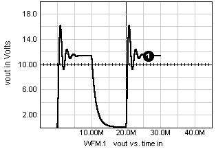
Figure 3-6: Buck Converter Turn-On and Turn-Off Versus Time
The turn-off waveform starts at 12 V and exponentially decays to zero volts without ringing. The cycle then starts again.
It is instructive to look at both of these events in the state-plane.
The state-plane, sometimes called the phase-plane, is a plot with two state-variables as coordinates. State-variables are variables whose initial conditions are required to determine the future behavior of the system. Typically they are anything that stores energy, like inductors and capacitors, or anything with a memory, such as a flip-flop. Common state-planes in switching-mode power supply design are inductor current versus capacitor voltage in the output LC filter (approximates load current and load voltage), the derivative of capacitor voltage (approximates the inductor current without the dc component) versus capacitor voltage, and the derivative of the output capacitor voltage versus the voltage (you do not have to be concerned with any currents and the derivative always crosses the voltage axis at right angles). Trajectories are unique for a set of initial conditions and never cross each other. Trajectories in the state-plane can easily be determined by most SPICE programs that are used to determine the time response of a circuit.
Figure 3-7 shows an approximate state-plane plot of the turn-on and turn-off events. The horizontal axis is the voltage across the output capacitor which approximates the output voltage. The vertical axis could one of several state-variables such as the inductor current, the derivative of the capacitor voltage, or the current through the capacitor. The inductor current, which approximates the load current is chosen. The steady-state turn-off conditions are 0 V and 0 A. The steady-state turn-on conditions are 12 V and 12 A (point one in the plot). The trajectories to reach these steady state conditions are shown in state-plane, Figure 3-7.
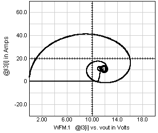
Figure 3-7: Buck Converter Turn-On and Turn-Off State-Plane
Turn-on
If there were no load, then the normalized turn-on trajectory would trace a clockwise circle reaching a positive peak current of Vin/Zo = (12 V)/(0.25 ohm) = 48 A, a peak voltage of twice the input voltage, 2*(12 V) = 24 V, and negative current equal to the positive current, return to zero volts, and then repeat itself until the circuit is disturbed, since there is nothing in the circuit that dissipates energy.
Since there is a load to dissipate energy, the circle spirals in to the steady state value of 12 V and 12 A (point 1) as energy is lost to the load or other dissipative elements as shown in Figure 3-7.
The state-plane turn-on trajectory tells us some things about this circuit that are worth remembering. On turn-on, buck-derived converters (and LC filters in general) tend to overshoot the final voltage, and can have an in-rush current much greater than the load current. Later in the design cycle it may be necessary to compensate for these inherent turn-on characteristics by adding soft-start circuits and in-rush current-limiting circuits to the design.
Also, the turn-on characteristics are dependent on the type of switch. In our ideal example, the switch can pass the inductor current in either direction, which is true of a relay contact or a power MOSFET, where the body parasitic diode will conduct current in the reverse direction. Other switches may not behave this way. For example, the reverse current behavior of a bipolar transistor depends on the reverse beta of the transistor and the base drive current. For old alloy junction transistors, the reverse and forward beta can be the same. For modern planar bipolar transistors, the reverse beta may be less than one and the transistor can carry only a small fraction of the forward current in the reverse direction. If the switch can not carry current in the reverse direction, the voltage rings up to the first peak and stays there until the load discharges it.
The bottom line is that you have to thoroughly know the behavior of the power switch to design reliable circuits. Later we will discuss switch topics such as secondary break-down, Safe Operating Areas (SOA), and parasitic elements that are important things to know about a switch. Here we see that it can be important to know how a switch behaves in quadrants other than its normal forward conduction quadrant.
Turn-off
The turn-of trajectory starts at 12 V and 12 A. The inductor keeps supplying 12 V to the load until it reaches zero amperes. Since the diode does not allow current to go below zero amperes, the voltage then drops along the zero ampere axis until it reaches its turn-off steady-state value of zero volts at zero amperes. There is no ringing in the waveform since the non-linear diode does not allow either voltage or current to go negative.
One easy way to turn our prototype buck converter into a 5 V regulator is to sense the output and turn the switch on when the voltage is less than 5 V and turn the switch off when the voltage is greater than 5 V. This form of control is called by various names including bang-bang control, ripple regulators, and hysteretic control. It is instructive to exam this operation in the state-plane. For the following plots the values of L and C are the same (75 uH and 1200 uF) but load is one ohm instead of 0.25 ohm (less damping shows the effects better).
Figure 3-8 shows bang-bang or hysteretic control with no hysteresis. The black line (1) is output voltage (voltage across the output capacitor) versus time, the blue line is inductor current (2) versus time, and the green line (3) is inductor current plotted versus capacitor voltage - the state plane for the two energy storage devices, L and C.

Figure 3-8: Bang-Bang Control - No Hysteresis
At time zero the switch representing the transistor is turned on and the voltage and current increase until the voltage reaches 5.0V. At this point the switch is turned off and the current starts to decrease. However, the voltage across the output capacitor continues to increase as long as current in the inductor is greater than the load current. The current drops to zero but does not reverse since the switch and diode will not allow this. When the voltage decays to 5.0V, the switch is turned again and voltage and current start to increase. This action is repeated with the amplitude of the voltage ripple and current ripple decreasing each cycle and the frequency increasing each cycle. In the limit the frequency becomes infinite and the ripple becomes zero and all that is left is a series dissipative regulator with an LC output filter. In this example, the initial cycle frequency is about 4.76 kHz, the voltage ripple is 30 mVp-p and the current ripple is 10Ap-p. This is seen on the state-plane in the outer limit of the green ellipse at (3). The ellipse is filled in as the ripple goes to zero and the frequency goes to infinity and we get a series dissipative regulator.
This we do not want. How do we keep things switching? By adding either a time delay in the control loop (time hysteresis) or voltage hysteresis in the comparator that senses the output voltage. In practice there is always some time delay in real components and the regulator may settle into some stable switching frequency. However, this is not dependable and a controlled delay or voltage hysteresis must be added.
Figure 3-9 shows the same circuit with a 1.2 microsecond delay added to the control loop.
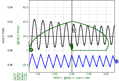
Figure 3-9: Bang-Bang Control - Delay Hysteresis
The 1.2 microsecond delay in the feedback loop has stabilized the frequency at about 12.5 kHz with 25 mVp-p voltage ripple and 3 Ap-p current ripple. However, the overshoot is just as bad as the circuit without hysteresis. (This is shown in the state plane but not the voltage and current time plots which show the steady state, not the start-up transient.) How do we cure this? With a soft-start circuit.
Figure 3-10 shows the startup with a soft-start circuit. The soft start is implemented in this case by slowly bringing up the reference voltage.

Figure 3-10: Bang-Bang Control with Soft Start Circuit
The red line (2) is the 5V reference voltage and ramps up from zero to 5V in 2 milliseconds. The black line (hidden 1) is the output voltage which follows the reference ramp except every time it makes a comparison to the reference and finds it is low, it turns on and overshoots the reference. At 2 ms it overshoots the desired 5V slightly and then after several oscillations settles into the steady state ripple. The green line (4) shows this action in the inductor-current versus output-voltage state plane.
Figure 3-11 shows the switching details during steady state conditions. The black line (1) is the output voltage ripple, the blue line (2) is the ripple current in the inductor, and the green line (3) is the ripple current versus the ripple voltage in the state-plane. To this has been a vertical red line added at the 5V switching line.
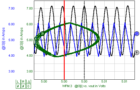
Figure 3-11: Switching Line Detail
When the upper green trace intercepts the red switching line, the comparator commands the switch to open. But due to the 1.2 microsecond delay added, the switching occurs some what later. The same with the lower green trace. This shows how the time hysteresis controls the output ripple and switching frequency (which is related in a somewhat complex way to the area traced by the trajectory). Note that although a time delay is used here, by putting two switching lines at the switch points (a comparator with voltage hysteresis) the ripple and frequency can be controlled by voltage hysteresis. Current hysteresis switching lines could also be used. Since all circuits have delays, the ripple and frequency are usually controlled by time delay and comparator hysteresis in real circuits. The switching line does not have to be fixed. For example, one converter uses as reference a fixed frequency triangle derived by chopping a dc reference and integrating the result into a triangle used as a reference for the comparator. This gives a fixed frequency of operation combined with the advantages of fast transient response and 90 degrees phase shift.
The state-plane is a very powerful way to look at switching-mode power supplies. For example, here we see a steady state response for one set of line and load conditions. Other sets of line and load conditions have their steady states. The state-plane can be used to find the optimum switching strategy between the two steady state conditions, optimum in that there is only one switching point that will allow a transition from one steady-state to the other steady state with a single off-on switching set. The state-plane has been used in this manner to determine optimum controllers for switching-mode power supplies. All modern Spice programs, including the free demonstration programs, allow plotting the state-plane and provide a powerful tool for examining switching-mode power supplies. I highly recommend looking at them as part of your simulation and using them to learn more about switching-mode power supplies. Ask yourself how does the state-plane change if I change the input voltage? How does it change if I change the load? What does the transition look like in the state plane for these changes. One caution is that you usually have to control the maximum step size to get smooth plots. Using the usual defaults for Spice time plots usually produces jagged state-plane plots. For the plots in this tutorial, I usually set the maximum step size to the data step time. This increases the time somewhat needed to complete a simulation but makes much cleaner state-plane plots.
Bang-bang control is very easy to implement. All circuits have a time delay, so a simple comparator comparing a reference to the output usually works -- and can always be made to work by adding an extra time delay. However, control is usually implemented using a comparator with hysteresis, hence the term hysteretic control. Whence the name bang-bang? This type of control is often used to control rocket and satellite control thrusters where a valve is either fully on or fully off. When tested in the atmosphere, these thrusters make a bang each time the are operated. When a control system is trying to lock on to a target, these thrusters can sound like the loudest machine-gun you have every heard. Definitely bang-bang!
Besides simplicity, bang-bang or hysteretic controllers only have 90 degrees phase shift which makes them easy to stabilize, and a rapid transient response. With these advantages, why do most power supplies use pulse-width-modulation (PWM) control instead? A minor reason is that hysteretic converters are more prone to chaos than other converters. But the major reason is their tendency to synchronize or entrain with a switching load, a periodic input voltage, or random noise -- often with unwanted or disastrous results, such as ripple on a five volt logic converter increasing from a tens of millivolts to several volts. All converters can do this, but bang-bang controllers are far more susceptible to this problem than PWM controllers. Entrainment will be discussed in detail in an upcoming problem/solution discussion.
Legal Statement
Do not use this information for design without independent verification of the information.
Copyright © 1999 - 2007 Jerrold Foutz
All Rights Reserved